Showing posts with label 555. Show all posts

Tuesday, November 18, 2014

555 timer calculator monostable and astable operation

This 555 timer IC calculator can calculate frequency, duty cycle, and high and low output of timer IC operation on both monostable and Astable. This Calculator script was written by Robert Davis of Goldsmith College
555 timer IC
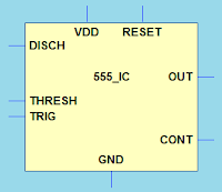
555 timer Pin number and designation:
pin 1- ground or common pin
pin 2- trigger pin
pin 3- output pin
pin 4- reset pin
pin 5- control pin
pin 6- threshold  pin
pin 7- discharge pin
pin 8- positive supply


555 MONOSTABLE OPERATION
Acts as one shot  pulse generator of output high duration of  T=RC ln(3)

555 timer monostable


R:


C:


T Output High (Seconds) =


555 TIMER ASTABLE OPERATION
555 timer astable operation


This operation has an output of continuous pulses of specified frequency and and duty-cycle.


R1:


R2:


C:


T1 Output High (Seconds) =


T2 Output Low (Seconds) =


T Total Period (Seconds) =


Frequency (Hz) =


Duty (%High) =
Read More..

Friday, October 3, 2014

Electronic circuit uses a 555

Electronic circuit uses a 555

The Electronic circuit uses a 555 timer wired as an astable oscillator and powered by the emitter current of the BC109C. Under dry conditions, the transistor will have no bias current and be fully off. As the probes get wet, a small current flows between base and emitter and the transistor switches on. A larger current flows in the collector electronic circuit enabling the 555 osillator to sound.


An On/Off switch is provided and remember to use a non-reactive metal for the probe contacts. Gold or silver plated contacts from an old relay may be used, however a cheap alternative is to wire alternate copper strips from a piece of veroboard.

These will eventually oxidize over but as very little current is flowing in the base circuit, the higher impedance caused by oxidization is not important. No base resistor is necessary as the transistor is in emitter follower, current limit being the impedance at the emitter (the oscillator circuit).
Read More..

Monday, September 1, 2014

555 Timer Long Time Delay Wiring diagram Schematic

This is a simple 555 Timer Long Time Delay Circuit Diagram. In the 555 timer, the timing is a function of the charging rate of the external capacitor. For long time delays, expensive capacitors with extremely low leakage are required. The practicality of the components involved limits the time between pulses to something in the neighborhood of 10 minutes. 
 

 555 Timer Long Time Delay Circuit Diagram

 
555
 
 
To achieve longer time periods, both halves of a dual timer may be connected in tandem with a `Divide-by`` network in between the first timer section operates in an oscillatory mode with a period of 1/fo. This signal is then applied to a `Divide-by-N` network to give an output with the period of N/fo. This can then be used to trigger the second half of the 556. The total time delay is now a function of N and fo.
Read More..

Thursday, August 28, 2014

Running Light circuit uses a CMOS 555 timer


A Transcutaneous Electrical Nerve Stimulation (TENS) device is, put bluntly, a machine for giving electric shocks. The author was prescribed such a device on loan by his orthopaedic specialist. The unit has a large number of programmes, of which he used only one. Measuring the signals at the output of the device in this mode revealed damped oscillations at a frequency of approximately 2.5 kHz, with a repetition rate of approximately 100 Hz.
Running
Running Light circuit uses a CMOS 555 timer

How hard can it be to make such a device ourselves? The simple circuit uses a CMOS 555 timer to produce a brief pulse which feeds a 1:10 miniature transformer. Together with a 4.7 nF capacitor the transformer makes a parallel resonant circuit: the resonance leads to a considerable increase in the output voltage. The pulse width can be adjusted using a potentiometer, here shown combined with the on-off switch. Wider pulses produce higher output voltages. Since a peak voltage of up to 200 V can be produced, the transformer must have adequate insulation: Conrad Electronics type 516260-62 is suitable. A low-cost phono socket at the output gives reliable connection to the electrode cable.

The adhesive electrodes shown in the photograph (disposable and permanent types are available) can be obtained from pharmacies and medical suppliers. They generally have connectors compatible with 2 mm banana plugs, and so it is possible to make up the necessary cable yourself. To treat responsive parts of the body, such as the arm, the potentiometer need not be turned up far to obtain the necessary sensation. Less sensitive parts, such as the knee or foot, need a rather higher voltage and hence a correspondingly higher potentiometer setting.

Author: Klaus Rohwer – Copyright: Elektor Electronics Magazine
Link:http://www.extremecircuits.net/2010/06/transcutaneous-electrical-nerve_03.html
Read More..

Wednesday, August 27, 2014

Using 555 as FM transmitter Wiring diagram Schematic

The integrated schema 555 has no limits, this FM transmitter schema, the IC 555 is designed as an stable multivibrator as usual. But the tension control pin is used to connect a piezoelectric element instead of the capacitor disk. The piezoelectric element generates a voltage and the output pin is connected to an antenna wire 30 inches for the transmission of signals.Just tap the piezo element and you can hear the sound on an FM radio station. The range is very short.


Using 555 as FM transmitter Circuit Diagram

Using

Read More..

Monday, August 25, 2014

Simple Water Sensor Wiring diagram Schematic using IC 555

This is a water sensor /rain alarm schema diagram; it can be used on motorcycle, car or other device that we want to protect from water, rain. This is a simple water sensor/rain alarm schema that makes an alarm when water/rain falls on its sensor. This schema is based on NE555/LM555 IC and two transistors (Q1&Q2). For transistor Q1- BC547 or BC107 and for Q2- 2N825,BC548 or BC168 can be used in the schema. 

This rain detector schema can be supplied from voltage source of +9V-12V DC. The resistor 470K ohm is a POT/Variable resistor; it is used to adjust the sensitivity of water/rain sensor. Use a 8 ohm,0.5w-1W speaker to hearing better alarm. Less than 8 ohm speaker could be harmful for the IC 555. 

Circuit Diagram of Water Sensor 

Simple

 We can make the water sensor as shown in the image (Fig-1) using aluminum conductor like a naked wire . Here can be used other conductor but we suggesting to use aluminum.
Read More..

Tuesday, August 19, 2014

Simple 555 Timer Circuit key cod

A very simple electronic key code lock schema that require few external components can be constructed using this schematic diagram . This electronic key code lock schema is based on a common 555 timer schema and some other common components .

This low cost key code schema use six switches that needs to be pressed to open the lock, but only two switches at a time. In many other , more expensive electronic diagram the key code is formed by pressing some switches one by one , not like in this case two switches . If you don’t like to press two switches in the same time you can eliminate one switch , but in that case the code can be more easy to guess by someone ells .Thus a total of three sets of switches have to be pressed in a particular sequence. (Of these three sets, one set is repeated.)

An essential property of this electronic code lock is that it works in monostable mode, i.e. once triggered, the output becomes high and remains so for a period of time, governed by the timing components, before returning to the quiescent low state.Pin 2 of 555 timer is the triggering input pin which, when held below 1/3 of the supply voltage, drives the output to high state. The threshold pin 6, when held higher than 2/3 of the supply voltage, drives the output to low state. By applying a low-going pulse to the reset pin 4, the output at pin 3 can be brought to the quiescent low level. Thus the reset pin 4 should be held high for normal operation of the IC.

Three sets of switches SA-SC, S1- S8 and S3-S4 are pressed, in that order, to open the lock. On pressing the switches SA and SC simultaneously, capacitor C3 charges through the potential
divider comprising resistors R3 and R4, and on releasing these two switches, capacitor C3 starts discharging through resistor R4. Capacitor C3 and resistor R4 are so selected that it takes about five seconds to fully discharge C3.


Depressing switches S1 and S8 in same time, within five seconds of releasing the switches SA and SC, pulls pin 2 to ground and IC 555 is triggered. The capacitor C1 starts charging through resistor R1. As a result, the output (pin 3) goes high for five seconds.Within these five seconds, switches SA and SC are to be pressed momentarily once again, followed by the depression of last code-switch pair S3-S4.

These switches connect the relay to output pin 3 and the relay is energised.
The contacts of the relay close and the solenoid pulls in the latch (forming part of a lock) and the lock opens. The remaining switches are connected between reset pin 4 and ground. If any one of these switches is pressed, the IC is reset and the output goes to its quiescent low state.
Read More..