 Source
Friday, October 31, 2014
Microphone FM Transmitter Wireless Two Transistors Circuit

Microphone FM Transmitter Wireless Two Transistors Circuit
Please be warned if operating this circuit might violate the regulation of your country, because this FM transmitter circuit radiate strong radio frequency to the environment. This wireless microphone is very sensitive, pick up every sound in the 20m radius, and transmit the radio signal up to 2 kilometers in open air. The first transistor (Q1) is the pre-amplifier for the microphone, and you can ommit this circuit if you don’t want to transmit the sound picked up by the mic, for example you can can connect your mp3 player directly to C1. The core of this FM transmitter circuit is Q2, a modified Collpits oscillator that the frequency is determined by L1, C4, C6, and the transistor’s internal base-emitter capacitance. The antenna use 1/16 wave length to compromize between the efficiency and the size.
If you want the microphone to be less sensitive, you can replace the R1 by a higher resistor, try 10k or 22k, and this might overcome the feedback problem if you use this wireless microphone FM transmitter for a public address system.
If you want the microphone to be less sensitive, you can replace the R1 by a higher resistor, try 10k or 22k, and this might overcome the feedback problem if you use this wireless microphone FM transmitter for a public address system.
Transistor Inverter circuit 12V to 220V 100W
This circuit power Inverter 100W, it easy and good ideas. When use the electric appliances that want 220V AC 50HZ, which have small-sized about 100Watt not exceed. By when you apply outside home, as a result have to have Mini power inverter about 100Watt, perform modify from work electricity forces of battery 12V give tall fair the work.

If you are New user electronics or want to economize or want to build electronics project use by oneself. I begs for to advise this circuit , because it uses , transistor number BC557 or the number replaces, perform oscillator generator. Then have power transistor 2N3055 numbers perform to drive coil transformer for converter voltage give tall go up 220V AC 50HZ at the electric power about 100 watt not exceed. When apply to transformer about 2A-3A.
Thursday, October 30, 2014
Mono to Stereo Audio Signal Circuit Converter
This circuit is used to convert a mono audio signal into a stereo signal that can be panned between the left and right channel by a 0-10V control signal, it is intended for analog synthesizer systems.
 |
| Circuit Convert Mono to Stereo Audio Signal Schematic |
Stereo PC Speaker Powered USB Speaker
This is the circuit diagram of USB powered computer speaker, or it widely known as multimedia speakers for PCs. The circuit has single-chipbased design, low-voltage electrical power supply, compatibility with USB power from computer, simple heat-sinking, inexpensive, large flexibility and wide temperature tolerance.
At the heart of the circuit is IC TDA2822M. This IC is, actually, monolithic type in 8-lead mini DIP (Dual Inline Package). It’s designed for use as a dual audio power amplifier in battery powered sound players. Features of TDA2822M are very low quiescent current, low crossover distortion, DC source voltage down to 1.8 volts and minimal output power of approximately 450 mW/channel with 4 ohm loudspeaker at 5V DC supply input.
An ideal power amplifier can be basically described as a circuit which can supply audio power into external loads without having producing substantial signal distortion and without having consuming extreme quiescent current.
This circuit is powered by 5V DC source obtainable from the USB port of the Computer. When electrical power switch S1 is turned to ‘on’ position, 5V power supply is extended towards the circuit and power indicator red LED1 illuminates immediately. Resistor R1 is actually a current surge limiter and capacitors C1 and C4 work as buffers.

How the circuit works..?
The operation of the circuit is very simple. Audio signals from the Computer audio port or headphone port are fed towards the amplifier circuit via R2 and C2 (for left channel), and R3 and C3 ( forright channel). Potensiometer VR1 used as the volume controller for left (L) channel, while potensiometer VR2 used to control the volume level of right (R) channel. Pin 7 of TDA2822M receives the left channel sound signals and pin 6 receives the right channel signals by way of VR1 and VR2, correspondingly. Amplified signals for driving the left and right loudspeakers can be obtained at pins 1 and pin 3 of IC1, correspondingly. Components R5 and C8, and R6 and C10 form the classic zobel network.
Construct the circuit on a medium size, general purpose PCB and enclose inside a appropriate case. It really is recommended to utilize a socket for IC TDA2822M. The external connections ought to be made working with suitably screened wires for improved result.
Dayton Amplifier SA1000
How Bridging Dayton Amplifier SA1000 - commonly used among the do-it-yourself passive subwoofer power. Amplifier, valued at close to 500 watts at eight ohms and over 900 in four Ohm, subwoofer driver capable of driving range. Bridging the amplifier to take the most power may sometimes desirable, depending on the individual needs of the audio.

Related searches :The things you need speaker wire strippers speaker wire banana plugs suggest edits Item added why does it need?Do
- Accessing back amplifier and found four clear plastic binding posts on rear panel.
- Strip 1/2 inch outer insulation of the cable end from the speaker to the subwoofer amplifier. Play a piece of wire tightly on each conductor.
- Remove the lower knurled button at the bottom of the banana plug. This shows the hole in the center of the plug body.
- Slide the speaker wire into the hole on a banana plug. Match the red wire to the red line on a banana plug. Repeat for the black wire and black striped banana plug.
- Slide the red wire into the hole below the end of the set of binding posts marked with a red strip. Repeat for the black wire.
Wednesday, October 29, 2014
Low voltage DC motor speed control circuit using TDA7274
Low voltage DC motor speed control circuit using TDA7274

Description.
Here is the circuit diagram of a low voltage /low power DC motor speed controller based on the IC TDA 7274 from ST Microelectronics. The IC TDA 7274 is a monolithic integrated DC motor speed controller intended for low voltage/ low power applications. Built in internal voltage reference voltage, wide input voltage range (1.8 t0 6V), high linearity, 700mA output current, excellent temperature stability etc make this IC well suitable for almost all low power DC motor speed control applications.
The motor to be controlled is connected between pin3 (Vs) and pin4 (output) of the IC. Resistor network comprising of R1, R2, and R3 is the section that deals with the speed control. Control pin (pin8) of the IC is connected to the junction of R2 and R3 and the speed of the motor varies linearly according to the position of POT R3. Capacitor C1 rectifies the fluctuations in motor speed and capacitor C2 cancels the motor spikes.
The circuit can be assembled on a Perf board.
Power supply Vs can be anything between 1.8V to 6V and it must be selected according to the rating s of the motor.
Maximum output current capacity of this circuit is 700mA.
TDA7274 must be mounted on a holder.
POT R3 can be used to vary the motor speed
RGB To Color Difference Converter Diagram Circuit
The circuit diagram shows two LT1398’s from Linear Technology used to create buffered color-difference signals from RGB (red-green-blue) inputs. In this application, the R input arrives via 75Ω coax. It is routed to the non-inverting input of amplifier IC1a and to 1.07-kΩ resistor, R8. There is also an 80.6-Ω termination resistor R11, which yields a 75-Ω input impedance at the R input when considered in parallel with R8. R8 connects to the inverting input of a second LT1398 amplifier (IC1b), which also sums the weighted G and B inputs to create a –0.5Y output.
![RGB]() Yet another LT1398 amplifier, IC2a, then takes the –0.5Y output and amplifies it by a gain of –2, resulting in the +Y output. Amplifier IC1a is configured for a non-inverting gain of 2 with the bottom of the gain resistor R2 tied to the Y output. The output IC1a thus results in the color-difference output R–Y. The B input is similar to the R input. Here, R13 when considered in parallel with R10 yields a 75-Ω input impedance. R10 also connects to the inverting input of amplifier IC1b, adding the B contribution to the Y signal as discussed above.
Yet another LT1398 amplifier, IC2a, then takes the –0.5Y output and amplifies it by a gain of –2, resulting in the +Y output. Amplifier IC1a is configured for a non-inverting gain of 2 with the bottom of the gain resistor R2 tied to the Y output. The output IC1a thus results in the color-difference output R–Y. The B input is similar to the R input. Here, R13 when considered in parallel with R10 yields a 75-Ω input impedance. R10 also connects to the inverting input of amplifier IC1b, adding the B contribution to the Y signal as discussed above.
![PSU]() Amplifier IC2b is configured to supply a non-inverting gain of 2 with the bottom of the gain resistor R4 tied to the Y output. The output of IC2b thus results in the color-difference output B–Y. The G input also arrives via 75-Ω coax and adds its contribution to the Y signal via resistor R9, which is tied to the inverting input of amplifier IC1b. Here, R12 and R9 provide the 75Ω termination impedance. Using superposition, it is straightforward to determine the output of IC1b. Although inverted, it sums the R, G and B signals to the standard proportions of 0.3R, 0.59G and 0.11B that are used to create the Y signal. Amplifier IC2a then inverts and amplifies the signal by 2, resulting in the Y output. The converter draws a current of about 30mA from a symmetrical 5-volt supply.
Amplifier IC2b is configured to supply a non-inverting gain of 2 with the bottom of the gain resistor R4 tied to the Y output. The output of IC2b thus results in the color-difference output B–Y. The G input also arrives via 75-Ω coax and adds its contribution to the Y signal via resistor R9, which is tied to the inverting input of amplifier IC1b. Here, R12 and R9 provide the 75Ω termination impedance. Using superposition, it is straightforward to determine the output of IC1b. Although inverted, it sums the R, G and B signals to the standard proportions of 0.3R, 0.59G and 0.11B that are used to create the Y signal. Amplifier IC2a then inverts and amplifies the signal by 2, resulting in the Y output. The converter draws a current of about 30mA from a symmetrical 5-volt supply.
Read More..
FM 250mW transmitter electronic Circuit diagram
A very simple FM transmitter electronic project can be designed using this circuit diagram . This FM transmitter electronic project works in FM band and it has a transmission power around 250mW ( thing that make it to work at above hundred meters ) . This FM transmitter electronic circuit is very simple and is based on some common transistors and electronic parts .
T1 transistor can be a BC107, BC171 or equivalent , and is used as an small audio preamplifier that amplify the audio signal from the microphone . Adjusting the R2 variable resistor, audio signal level from the input ( microphone ) can be adjusted until will be delivered to the T1 preamplifier (an over amplified signal applied to T1 can produce an overmodulation) . From T1 , signal is delivered to T2 which form an Hartley oscillator (frequency of this oscillator depends of C8,C9 and L1) .
 The transmitter frequency oscillator works in FM band 87.5-108 MHz and can be set , adjusting C8 capacitor and L1 coil . L1 coil must have four turnings on a 0.8-1 mm cylinder support with a 6 mm diameter (space between each wire must be around 1 mm ) .
Antenna used for this project can be a simple telescopic antenna or a 60-70 mm Cu wire .
This electronic project can be powered from a wide range input voltage from 9 to 12 volts Dc ( but can be used even a 18 volts DC .
T1 transistor can be a BC107, BC171 or equivalent , and is used as an small audio preamplifier that amplify the audio signal from the microphone . Adjusting the R2 variable resistor, audio signal level from the input ( microphone ) can be adjusted until will be delivered to the T1 preamplifier (an over amplified signal applied to T1 can produce an overmodulation) . From T1 , signal is delivered to T2 which form an Hartley oscillator (frequency of this oscillator depends of C8,C9 and L1) .
Antenna used for this project can be a simple telescopic antenna or a 60-70 mm Cu wire .
This electronic project can be powered from a wide range input voltage from 9 to 12 volts Dc ( but can be used even a 18 volts DC .
Tuesday, October 28, 2014
LMP91000 Chemical Gas Sensors
Chemical & gas Sensors
Read More..
The LMP91000 low-power swap gossip and compound Sensor AFE provides flexible bias (sensor drive), sensitivity, and ample dynamic range happening an integrated solution in support of multiple sensing applications. For case, a toxic chatter sensing diligence with the purpose of now could require several boards and up to 25 components is concentrated to a moment ago individual LMP91000 chatter sensor AFE.
 |
| lmp91000 chemical gas sensors. |
- Single analog design meant for multiple gases and chatter concentrations
- Programmable cell bias and TIA reward
- Integrated heat sensor for exterior temp monitoring / correction
- Quick design and evaluation
- Ideal for micro-power chatter and element sensing applications
Datasheet LMP91000 - Download - Product Detail
Audio Distribution Amplifier
With the amount of equipment indoors domicile entertainment centers in our day the need to live able to vary the improvement of the audio otherwise capture signify is desired. I found this meticulous circuit obliging while used in conjunction with the Universal Descrambler and a Stabilizer circuit I built intended for making copies of capture on tape tapes. It not solitary permissible me the capability to fine regulate the video strength it moreover helped me growth the recorded audio which typically becomes poor once making tape copies. Circuit function is straight into the open intended for amplifier circuits. The back up channel for the audio amplifier is made up of the same components aside from the other partially of IC1 is used. Pin 6 & 5 are inputs and 7 is the output.
 |
| Audio Distribution Amplifier |
Monday, October 27, 2014
Vertical IC Configuration
Various kinds of vertical out IC configuration. Ac coupling -connect from the yoke deflection output to a coil connected directly. Dc coupling - connected the output to the coil through a capacitor deflectioan yoke. Electrolityc Capacitors (usually worth 1000u/35v). This configuration requires two kinds of voltage (the voltage mirror plus-minus). Dc input coupling using diffferential - uses 2 input from the driver IC.
 |
| Vertical IC Configuration AC Coupling |
 |
| Vertical IC Configuration DC Coupling |
BA5406 10W Stereo Power Amplifier
BA5406 is a monolithic integrated stereo amplifier from ROHM semiconductors. It can transfer 5W apiece channel into a 4 ohm loudspeaker by the side of 9V supply. Amplifiers based on BA5406 does not require an output coupling transformer and can subsist operated from a single supply. The operating voltage range is from 5 to 15V DC. This makes the IC correct in lieu of low power car audio applications. Other applications of BA5406 are portable audio players, stereo module systems, television and all that. The BA5406 has important channel separation, excellent channel isolation, unimportant pop-up clatter, low noise, low thermal resistance and is open arrived a 12 pin SIP package.
Read More..
 |
| BA5406 10 Watt Stereo Power Amplifier |
In the circuit diagram revealed lower, BA5406 is configures to hand over 5×2 watts into 4 ohm loudspeakers by the side of a supply voltage of 9 volts. Capacitor C3 is a power supply filter capacitor. C11 and C12 are input DC decoupling capacitors on behalf of the missing and due channels. C3 and R2 forms a Zobel arrangement for the not here output while C6 & R3 forms the same for the right channel. single-mindedness of the Zobel network is to reduce oscillations and rally in height frequency stability of the amplifier. Potentiometers R5 and R6 serves since the volume control on behalf of the not here and right channels. CapacitorsC4 and C8 pair the outputs of the amplifier to the speakers. C9 and C10 are clamor filtering capacitors. C1 and C5 are bootstrap capacitors for the not here and right channels.
Sunday, October 26, 2014
LM1875 80W audio power amplifier Diagram Circuit
A very simple high efficiency 80W audio power amplifier project can be designed using the LM3875 power audio IC . LM3875 is a high-performance audio power amplifier capable of delivering 56W of continuous average power to an 8Ω load with 0.1% THD+N from 20Hz to 20kHz .
By connecting two LM39875 audio IC in bridge mode this audio power amplifier will deliver 80 watt of output power into an 8 Ohm load. The LM3875 IC devices should be suitably heatsinked.
As you can see in the circuit diagram , this power audio amplifier require few external electronic parts .
The LM3875 maintains an excellent signal-to-noise ratio of greater than 95dB(min) with a typical low noise floor of 2.0μV.
This 80W audio power amplifier module accepts a wide range input voltage from 20 up to 84 volts, but typically is recommended ( for this circuit ) a dual +/-25 volts DC power supply .
Some features of this 80W audio power amplifier project based on the LM1875 IC are :
output protection from a short to ground or to the supplies via internal current limiting circuitry ,output over-voltage protection against transients from inductive loads ,supply under-voltage protection .
Diagram rossover types
Crossover is a tool that serves to limit the "frequency range" to be received by the speaker. Crossover is used to regulate flow to the tweeter, the midrange, midwoofer, and bass to the subwoofer. There are two kinds of crossover, the crossover passive and active crossover.
 |
| passive crossover |
Passive crossovers work after receiving the output of the amplifier, are ineffective because they are throwing power amplifier, because the passive crossover frequencies have been processed in the "boost" (increase) by the amplifier.
 |
| active crossover |
Active crossovers work so signal generated by the head unit (pure signal), dividing it in accordance with the desired frequency boost later in the amplifier, so that the amplifier to work more efficiently, and frequencies produced more organized in accordance with their respective purposes, tweeter, midrange, woofer , subwoofer.
A little short in the use of an active crossover is the use of 12V power, ground, and remote. In theory this could lead to "noise" on the audio system, but do not worry, by the proper installation, and use good quality products will not occur a problem, as in any "competition-level car audio system". If you want to raise just a little audio sound quality, passive crossover is the right choice. But if want the sound quality is really good you should select an active crossover. Active crossovers require special mounting, especially for power cables and ground wires, but the effort is proportional to the quality of music produced. Active Crossover works by "cutting" is not frequency necessary before the "boost" by the amplifier, so the amplifier can focus on the frequency you want to hear, so do not waste energy Power.
Saturday, October 25, 2014
Stereophonic circuit with TDA7088T
There are two signals that are directed at the so-called FM transmitter the coder (coding). Multiplexing Mpx signal has been contained, two left signals and right indirectly. Frequency modulation of a transmitter carried by the signal Mpx. The receiver output signal is obtained on Mpx and FM detector is then passed to the decoder. At the decoder do the opposite with the coder in the transmitter, because at this level produced two signals L and D.

Signal is amplified by audio amplifier dientik two, then reproduced through two speakers are the same. Now listeners can heard coming from the left half the loudspeaker is placed on the left and right half of which is placed on the right side. Situation amid the orchestra will be equal to that of the second lordspeaker reproduced, made an impression on the listener as if there.
The third loudspeaker placed midway between the left and right. Based on all these listeners have a picture of the layout space, which is significantly increased total musical impression. Electronic circuits of the portable stereophonic radio receiver with headphones reproduction, made by the IC TDA 7088T is shown in Figure the above. This is a practical embodiment of the receiver with TDA7040T decoder and two audio amplifier with TDA7050T IC.
Choke (coils) L3, L4 and L5 are HF coil allows the headphone cable is used as a receiving antenna. this fulfilled by connecting one contact of the plug-in headphones, through a 10 pF capacitor at the point where the output of the antenna is connected. Coil has a significant barrier to the signal station, preventing ground connection through capacitor 47 mF or through the TDA7050T output.
Friday, October 24, 2014
3 Band Tone Control Circuit
3 Band Tone Control circuit uses an op-amp as an amplifier end. Tone Control circuit is a regulator of tone bass, midrange and treble or 3 band called because it can set the three tones. Filter circuit is applied to the series of "Tone Control 3 band" This type baxandal like the title of this article.
Results filtering regulator tone or tone control baxandal type is good, because there is no signal level is wasted directly into the ground. Range frequency tones generated from Tone Control 3 band was determined by the configuration of the R and C of the filter section baxandal. As an amplifier on Tone Control The set of three band use traditional IC LF351 has slewrate high and high input impedance. For more details, series 3 Band Tone Control as follows.
Figure Series 3 Band Tone Control

Thursday, October 23, 2014
Diagram Running LED with 4017
Running LED with 4017 complete with PCB layout. The series of 8 LED current is the basis for creating an 8-point LED. Slightly different from the running LED with IC 4017 (decade counter), 8 running this led is lit in sequence, but that has been previously flame does not die when the led is lit afterwards. 8 led to death after led to the fire-8. Meanwhile in the running LED (decade counter), the system LED lights like "point", there is only one LED that flashes between the tenth led.

The main component is the IC 74LS164 (SHIFT REGISTER), with its timer is astable multivibrator circuit (using IC NE555).
The series will be more efficient when using a stable power supply (regulator) using IC Regulator 7805. Under this scheme a series of stable power supply 5 volts dc.

Transceiver Homebrew QRP SSB 80M Band
Radio communication transceiver is a radio transmitter at the same time the plane doubles as a radio receiver used for communication purposes. It consists of the transmitter and the receiver are assembled in an integrated way. In mulamula generation, the transmitter or receiver or transmitter and receiver sections are assembled separately and is part of a stand sendirisendiri and can work well Currently employed both parts are integrated in turn.
 Aircraft simple transmitter consists of an oscillator generating radio vibration and this vibration after vibration boarded with our voice, in a technique called dimodulir radio, then by the antenna is converted into radio waves and transmitted. As we know that the sound waves we can not reach long distances, although its power is quite large, while the radio waves with a relatively small force can reach a distance of thousands of kilometers. In order for our voice can reach a far distance, then our voice superimposed on radio wave radio results from the vibration generator, called a carrier wave or carrier and the carrier wave was going to deliver our voice to distant places.
In a place far earlier, the radio waves emitted by the antenna received our speaker. By the antenna, radio waves had, in the form of electromagnetic waves is converted into electrical vibrations and into the receiver.
In our speaker receiver plane, vibration and vibration carriernya then discarded and then raised our voices be accommodated through the speakers. With this technique it is possible modilasi an audio vibrations reach a far range.
We sound vibrations enter the transmitter through a microphone, microphone output was often needs to be strengthened first with an audio amplifier is called a microphone preamplifier can be superimposed on the carrier for the modulator.
To increase the transmission power of a transmitter, vibration of the oscillator was before the emitted amplified first with a radio frequncy amplifier. Strengthening can be done once and can also be done more than once. Transmitter is not reinforced is called a level transmitter and the reinforced one called two-level and beyond. In general, to reach 100 Watt transmit power need to strengthen the 3 times, the first amplifier is called predriver, the next amplifier called the driver and final amplifier called the final amplifier.
Block Diagram of SSB Transceiver
If were talking about the Single Side Band, then we touched more on amplitude modulation (AM). At each modulation we do we actually do the mixing between the radio frequency to audio frequency. Any mixing of two frequencies will occur the second summation process and at the same frequency reduction process occurs from both frequencies.
So every time we memodulir carrier, will produce two frequencies at once. For example, a carrier with a frequency of 3000 Kc we modulir with audio ferkuensi 3 Kc, the result is 3003 Kc and Kc 2997, or said occurred two sides of the band is the upper side and lower side. The top side and bottom side are shaped symetris, so if it is a direct result of modulation we mean we memancarakan exude the same two goods.
If we shine the way mentioned above, we use the mode is said to Double Side Band (DSB) because the carrier that includes top and bottom sides are emitted together. In factory-made plane, this mode is usually coded in terms actual AM radio is the DSB technique.
We know there are two kinds of ways to make the SSB, the first way is by phase shift method, another way is by filtering methods. The first way is not widely used and factory-made aircraft SSB generally use filtering.
Signal DSBSC, before the amplified and transmitted, is inserted into the SSB filter in advance to produce LSB or USB. Filters are used for this purpose is filtering crystal or mechanical filters. SSB transmitter is said to be more efficient than AM (DSB), we can give this picture as follows. For example transmitter AM (DSB) with power 150 Watt (100% modulation depth), then power on the USB and LSB respectively and the carrier has a 25 Watt 100 Watt power. We know that the audio side we are on the band. In the SSB emission, emitted only one side band LSB or USB is a powernya only 25 Watt.
With SSB 25 Watt beam, the audio we have to arrive at destination with the same clarity of information with jet AM (DSB) 150 Watt earlier.
Another advantage of SSB is the wide-band mode that can be more narrow. For the purposes of communication, SSB mode requires only the band width of about 3 Kc, while the DSB mode takes about 6 Kc, thus providing savings SSB mode the use of the band.
In the detector a SSB receiver, the received signal must be mixed in advance with the frequency of the outcome of a Beat Frequency Oscillator (BFO) and used as the BFO carrier oscillator.
Homebrew QRP SSB Transceiver circuit 80m Band
In general, the transceiver has the following block diagram, basically Transceiver tebagi into three main parts: Part VFO and BFO Part Transmitter (transmitter) and Section Receiver (receiver), where there are some special blocks that are used for both paths are either transmitter or receiver. Simply in this transceiver merkit Use the tools that we only Multi tester, RF Probe, SWR and Power Meter, Tone Generator Af 1Kc and multi-band Radio HF SSB to function as a monitor frequency BFO, VFO, monitor Balanced Modulator Exciter at once both the transmitter or receivers .
Data Transceiver:
Frekwency Range: 3700 Kc a / d 3900 Kc
Mode: LSB Singgle conversi
IF: 455 Kc (Ceramic Filter SFU type 455)
Local oscillator: VFO with Fine Tuning varactor diode
BFO: Ceramic Filter 455 SFU
RF PA: Power FET IRF640, IRF540, IRFZ44
DC: 13.8 V
RF Power: Over 8Watt
Description Schema.
The order of assembly sequence of assembling consecutive start BFO, VFO, AF Amp, IF amplifier and detector products to filter amplifier circuit, Mic Amplifier, Balanced modulator, RX mixer + Rf amplifier, mixer TX last order to facilitate the checking of each unit due to series This is a merger of several units of its own circuit.
BFO.
using SFU type ceramic filters used 455 two-foot middle leg to ground is coupled with capacitor and capacitor trimer and one leg edges to the base of the transistor, BFO uses two types of 2SC1815 transistors. Tc 1 to set the BFO on 453.5Kc frekwensy being black 455Kc IF transformer to regulate the level rather than BFO. To check this The set uses RF Probe. At the secondary BFO output T9 check with RF probe set T9 smpai maximum output level monitor in the radio frequency or HF trimer and Counter set Capacitor capacitor pararelnya until fulfilled the required frequency of 453.5Kc. To check whether there are oscillations in the BFO off Ceramik filter whether RF probe was still moving when he checks it again rangakain ceramik here if we filter out the RF probe is not moving.
VFO.
For we use the VFO FET 2SK192 Type and reinforced with a single fruit type transistor 2SC1815. Raft of this series as neat munkin with component selection, especially capacitor here we use a paper capacitor in series of Colpits oscillator. Close this series with a metal box along with all Varconya. VFO same testing with the BFO circuit Trime Koker Ferrite T13 dapakan frequency monitor the frequency of 4100 Kc s / d 4300 Kc obtained in case of no frequency range is set set the number of coil and capacitor values bypas tothe ground.
AF amplifier.
AF Amplifier IC type LM386 used raft this section and check out by Spiker at putnya. Plug the foot of its inputs with a screwdriver had no defects at the time vulume potensio enlarged.
IF AMP AND PRODUCT detector.
Raft had Produc detectornya from starting until the fourth diode 1N60 IF transformer T7 455 black color until the transformer bypass capacitor to ground. Plug one side of the transformer with a screwdriver kai harden the audio volume on the speakers should be no reaction. Attach the amplifier transistor for testing at its base on the speaker should be louder voice. Raft this section everything.
FILTER amplifier.
Put all the components properly to eighth ceramic filter installed all. Just listen to the speaker plug on the input or pairs if a small number of meters of cable serves as an antenna trim T6 and T8 listen to the voice on the speaker until no defects dispeaker be hissed loudly.
RX MIXER AND RF amplifiers.
This series of rafts with the good and right in making the winding must be in a state of neat. Enter Snyal VFO to try to monitor the input mixer is QSO friends turn ferrite in successive Koker turu of T3 and T4 to get a strong signal reception and set the T1 and T2 ferrite to signal strong receipts received with respect to the level of the S Meter. If that is not found try to check this section further. Thus selesei weve Section Receiver unit.
MIC amplifier.
Raft of this section and replace all the LM 741 IC listen with headphones turn out putnya potensio putnya try out the level of talk in the microphone must be perfect without any defects in the out put
BALANCE modulator.
Balanced modulator uses AN612 ic type commonly used on the CB radio. Raft all components correctly. To check this series of pairs of probes to the output at ic AN612 when no signal on the IC probe set trimpot until the deviation of zero and then try to plug in with tweezers pda mic input amplifier should have needle probe deviation. Then plug micropon try talking meter on the probe to move the motion according to your speech input level. Put some small cable length as the antenna you are trying to monitor diradio HF signal here was DSB Uper and Lower Side band sound. Dengarka until there is no defect here is selesei sets. Then go Filter amplifier output to try to talk Rangkian denagan put up some yards kabbel to secondary T6 try IF 455 White color monitor frequency of 455 Kc diradio on and try to talk trim ferrite Ferrite T6 and T8 until you hear the sound on USB diradio no oscillation and no deviation selef the meter on the probe. If on your radio monitors have didapatka perfect sound means youve selesei at once to part If rceifernya.
TX MIXER.
Raft section make this all too well circumference at T11 and T12 as neat as possible. Mixer that we use the type of premises IC TA7310 2SC1815 transistor amplifier pairs as well. Then plug VFO output and Out put Balnce Modulatornya on laulu TA7310 ic input probe pairs give the mic input with tone generator af ferrite trim T11 and T12 refer to deviation meter probe to obtain the largest deviation meter. Put microppon try talking dimicropon deviation meter see if were not talking micropon but no deviation on the meter needle probe set trim T11 and T12 until no deviation in meters try to talk again in micropon deviation meter should move according to their level talks on the microphone. Try installing a few meters of the small wires on the monitor amplifier output tx diradio exciter in accordance with the frequency of our work with the fashion side band LSB if we do not get on the LSB mode with sempurana set again trimer capacitor on the BFO and rotate slightly if T8 transformer ferrite in black color smpai obtained side band we want. Up here seleseilah exciter circuit.
TX PA amplifier.
PA series we take the type of Power FET because it is cheap and easily available in the market. Create a transformer with a good and right not to email pda scuffed pair of wires until there is a first level transistor 2SC1815 output pairs of probes on trying to talk on the microphone deviation at Beh probe must be greater than the level of exciter here should not happen if not self-oscillation oscillation talk there is no deviation on the meter needle probe. In the event of self-oscillation try to check the part. Similarly, the driver assembly. Drivers are taking transistor type 2 SC1162. gained power level meter must be greater than the previous level as well. Then the final units also make coils as neat as possible. Testing out first input of the exciter arur Pa measuring voltage trimpot should not exceed 3V plug out put a probe hyarus no deviation on the meter. In the event of significant deviation occurs in pagian the oscilasi cell. Then plug the input of the exciter ac voltmeter pairs of avo meter try to speak in micropon meter on ac at avo meter should show a few volts ac in accordance with the level of talking on the microphone.
LOW PASS FILTER.
Create a winding low pass filter with a nice and neat L1 and L2. pairs of all components of the relay to properly check penyambunngan pairs dumy 50 Ohm load at the antenna output connector do not forget to SWR and Power meter is installed. Speaking at a microphone set set ferrite Koker L1 and L2 to obtain the maximum and then check SWR poiwer it must appoint 1: 1 with dumy Load 50 ohms if not check again Low Pass filters. After iti try to plug the 80m band antenna connector is on your monitor qrp radio QSO friends who try to enter it and asked for the report
Read More..

In a place far earlier, the radio waves emitted by the antenna received our speaker. By the antenna, radio waves had, in the form of electromagnetic waves is converted into electrical vibrations and into the receiver.
In our speaker receiver plane, vibration and vibration carriernya then discarded and then raised our voices be accommodated through the speakers. With this technique it is possible modilasi an audio vibrations reach a far range.
We sound vibrations enter the transmitter through a microphone, microphone output was often needs to be strengthened first with an audio amplifier is called a microphone preamplifier can be superimposed on the carrier for the modulator.
To increase the transmission power of a transmitter, vibration of the oscillator was before the emitted amplified first with a radio frequncy amplifier. Strengthening can be done once and can also be done more than once. Transmitter is not reinforced is called a level transmitter and the reinforced one called two-level and beyond. In general, to reach 100 Watt transmit power need to strengthen the 3 times, the first amplifier is called predriver, the next amplifier called the driver and final amplifier called the final amplifier.
Block Diagram of SSB Transceiver
If were talking about the Single Side Band, then we touched more on amplitude modulation (AM). At each modulation we do we actually do the mixing between the radio frequency to audio frequency. Any mixing of two frequencies will occur the second summation process and at the same frequency reduction process occurs from both frequencies.
So every time we memodulir carrier, will produce two frequencies at once. For example, a carrier with a frequency of 3000 Kc we modulir with audio ferkuensi 3 Kc, the result is 3003 Kc and Kc 2997, or said occurred two sides of the band is the upper side and lower side. The top side and bottom side are shaped symetris, so if it is a direct result of modulation we mean we memancarakan exude the same two goods.
If we shine the way mentioned above, we use the mode is said to Double Side Band (DSB) because the carrier that includes top and bottom sides are emitted together. In factory-made plane, this mode is usually coded in terms actual AM radio is the DSB technique.
We know there are two kinds of ways to make the SSB, the first way is by phase shift method, another way is by filtering methods. The first way is not widely used and factory-made aircraft SSB generally use filtering.
Signal DSBSC, before the amplified and transmitted, is inserted into the SSB filter in advance to produce LSB or USB. Filters are used for this purpose is filtering crystal or mechanical filters. SSB transmitter is said to be more efficient than AM (DSB), we can give this picture as follows. For example transmitter AM (DSB) with power 150 Watt (100% modulation depth), then power on the USB and LSB respectively and the carrier has a 25 Watt 100 Watt power. We know that the audio side we are on the band. In the SSB emission, emitted only one side band LSB or USB is a powernya only 25 Watt.
With SSB 25 Watt beam, the audio we have to arrive at destination with the same clarity of information with jet AM (DSB) 150 Watt earlier.
Another advantage of SSB is the wide-band mode that can be more narrow. For the purposes of communication, SSB mode requires only the band width of about 3 Kc, while the DSB mode takes about 6 Kc, thus providing savings SSB mode the use of the band.
In the detector a SSB receiver, the received signal must be mixed in advance with the frequency of the outcome of a Beat Frequency Oscillator (BFO) and used as the BFO carrier oscillator.
Homebrew QRP SSB Transceiver circuit 80m Band
In general, the transceiver has the following block diagram, basically Transceiver tebagi into three main parts: Part VFO and BFO Part Transmitter (transmitter) and Section Receiver (receiver), where there are some special blocks that are used for both paths are either transmitter or receiver. Simply in this transceiver merkit Use the tools that we only Multi tester, RF Probe, SWR and Power Meter, Tone Generator Af 1Kc and multi-band Radio HF SSB to function as a monitor frequency BFO, VFO, monitor Balanced Modulator Exciter at once both the transmitter or receivers .
Data Transceiver:
Frekwency Range: 3700 Kc a / d 3900 Kc
Mode: LSB Singgle conversi
IF: 455 Kc (Ceramic Filter SFU type 455)
Local oscillator: VFO with Fine Tuning varactor diode
BFO: Ceramic Filter 455 SFU
RF PA: Power FET IRF640, IRF540, IRFZ44
DC: 13.8 V
RF Power: Over 8Watt
Description Schema.
The order of assembly sequence of assembling consecutive start BFO, VFO, AF Amp, IF amplifier and detector products to filter amplifier circuit, Mic Amplifier, Balanced modulator, RX mixer + Rf amplifier, mixer TX last order to facilitate the checking of each unit due to series This is a merger of several units of its own circuit.
BFO.
using SFU type ceramic filters used 455 two-foot middle leg to ground is coupled with capacitor and capacitor trimer and one leg edges to the base of the transistor, BFO uses two types of 2SC1815 transistors. Tc 1 to set the BFO on 453.5Kc frekwensy being black 455Kc IF transformer to regulate the level rather than BFO. To check this The set uses RF Probe. At the secondary BFO output T9 check with RF probe set T9 smpai maximum output level monitor in the radio frequency or HF trimer and Counter set Capacitor capacitor pararelnya until fulfilled the required frequency of 453.5Kc. To check whether there are oscillations in the BFO off Ceramik filter whether RF probe was still moving when he checks it again rangakain ceramik here if we filter out the RF probe is not moving.
VFO.
For we use the VFO FET 2SK192 Type and reinforced with a single fruit type transistor 2SC1815. Raft of this series as neat munkin with component selection, especially capacitor here we use a paper capacitor in series of Colpits oscillator. Close this series with a metal box along with all Varconya. VFO same testing with the BFO circuit Trime Koker Ferrite T13 dapakan frequency monitor the frequency of 4100 Kc s / d 4300 Kc obtained in case of no frequency range is set set the number of coil and capacitor values bypas tothe ground.
AF amplifier.
AF Amplifier IC type LM386 used raft this section and check out by Spiker at putnya. Plug the foot of its inputs with a screwdriver had no defects at the time vulume potensio enlarged.
IF AMP AND PRODUCT detector.
Raft had Produc detectornya from starting until the fourth diode 1N60 IF transformer T7 455 black color until the transformer bypass capacitor to ground. Plug one side of the transformer with a screwdriver kai harden the audio volume on the speakers should be no reaction. Attach the amplifier transistor for testing at its base on the speaker should be louder voice. Raft this section everything.
FILTER amplifier.
Put all the components properly to eighth ceramic filter installed all. Just listen to the speaker plug on the input or pairs if a small number of meters of cable serves as an antenna trim T6 and T8 listen to the voice on the speaker until no defects dispeaker be hissed loudly.
RX MIXER AND RF amplifiers.
This series of rafts with the good and right in making the winding must be in a state of neat. Enter Snyal VFO to try to monitor the input mixer is QSO friends turn ferrite in successive Koker turu of T3 and T4 to get a strong signal reception and set the T1 and T2 ferrite to signal strong receipts received with respect to the level of the S Meter. If that is not found try to check this section further. Thus selesei weve Section Receiver unit.
MIC amplifier.
Raft of this section and replace all the LM 741 IC listen with headphones turn out putnya potensio putnya try out the level of talk in the microphone must be perfect without any defects in the out put
BALANCE modulator.
Balanced modulator uses AN612 ic type commonly used on the CB radio. Raft all components correctly. To check this series of pairs of probes to the output at ic AN612 when no signal on the IC probe set trimpot until the deviation of zero and then try to plug in with tweezers pda mic input amplifier should have needle probe deviation. Then plug micropon try talking meter on the probe to move the motion according to your speech input level. Put some small cable length as the antenna you are trying to monitor diradio HF signal here was DSB Uper and Lower Side band sound. Dengarka until there is no defect here is selesei sets. Then go Filter amplifier output to try to talk Rangkian denagan put up some yards kabbel to secondary T6 try IF 455 White color monitor frequency of 455 Kc diradio on and try to talk trim ferrite Ferrite T6 and T8 until you hear the sound on USB diradio no oscillation and no deviation selef the meter on the probe. If on your radio monitors have didapatka perfect sound means youve selesei at once to part If rceifernya.
TX MIXER.
Raft section make this all too well circumference at T11 and T12 as neat as possible. Mixer that we use the type of premises IC TA7310 2SC1815 transistor amplifier pairs as well. Then plug VFO output and Out put Balnce Modulatornya on laulu TA7310 ic input probe pairs give the mic input with tone generator af ferrite trim T11 and T12 refer to deviation meter probe to obtain the largest deviation meter. Put microppon try talking dimicropon deviation meter see if were not talking micropon but no deviation on the meter needle probe set trim T11 and T12 until no deviation in meters try to talk again in micropon deviation meter should move according to their level talks on the microphone. Try installing a few meters of the small wires on the monitor amplifier output tx diradio exciter in accordance with the frequency of our work with the fashion side band LSB if we do not get on the LSB mode with sempurana set again trimer capacitor on the BFO and rotate slightly if T8 transformer ferrite in black color smpai obtained side band we want. Up here seleseilah exciter circuit.
TX PA amplifier.
PA series we take the type of Power FET because it is cheap and easily available in the market. Create a transformer with a good and right not to email pda scuffed pair of wires until there is a first level transistor 2SC1815 output pairs of probes on trying to talk on the microphone deviation at Beh probe must be greater than the level of exciter here should not happen if not self-oscillation oscillation talk there is no deviation on the meter needle probe. In the event of self-oscillation try to check the part. Similarly, the driver assembly. Drivers are taking transistor type 2 SC1162. gained power level meter must be greater than the previous level as well. Then the final units also make coils as neat as possible. Testing out first input of the exciter arur Pa measuring voltage trimpot should not exceed 3V plug out put a probe hyarus no deviation on the meter. In the event of significant deviation occurs in pagian the oscilasi cell. Then plug the input of the exciter ac voltmeter pairs of avo meter try to speak in micropon meter on ac at avo meter should show a few volts ac in accordance with the level of talking on the microphone.
LOW PASS FILTER.
Create a winding low pass filter with a nice and neat L1 and L2. pairs of all components of the relay to properly check penyambunngan pairs dumy 50 Ohm load at the antenna output connector do not forget to SWR and Power meter is installed. Speaking at a microphone set set ferrite Koker L1 and L2 to obtain the maximum and then check SWR poiwer it must appoint 1: 1 with dumy Load 50 ohms if not check again Low Pass filters. After iti try to plug the 80m band antenna connector is on your monitor qrp radio QSO friends who try to enter it and asked for the report
Wednesday, October 22, 2014
Flip Flop Led Circuit
Flip flop circuit is a series of free runing multivibrator given the burden of LEDs on each side of the transition changes its output signal. Flip flop circuit with LEDs is quite simple, that is prepared with 2 units and 2 units of 2N3904 transistor circuit tank circuit composed by the RC circuit.
LED indicators signal a change that is placed on each side of the flip flop will be lit in turn by the fire and extinguished the same as the charge and discharge capacitor. Flip flop circuit is quite simple as shown in the picture below.

Flip Flop LED series
The working principle is the flip flop over when the series voltage source is given then the 10uF capacitor will be charged through R 470 and the LED will then be forwarded to triger the transistor base so that the transistor will turn ON and LEDs. this occurs alternately on each side, so that the LED light will illuminate in turn as well.
Sunday, October 19, 2014
Basically the DAC circuit
Since the discovery of Silicon and Germanium semiconductor material then quickly there was a revolution in terms of simplicity and accuracy of an electronic circuit. Besides, with the implementation of digital circuits will support at all in terms of data storage and mobility. Lots of data can now be operated with a computer is a data converted from analog signals. For example a voice signal or analog form of video can be played and stored using a computer after analog signals are converted into digital data.
 Advantages possessed by the digital data than analog signal is a certainty the nature of the data or logic. Digital data only can be divided into two kinds of logic high "1" and logic low "0". Logic 1 represents 5 volts and low logic voltage 0 volts represents. Examples of the advantages of digital signals over analog signals is on television or digital radio receiver. By implementing a digital system signals emitted by television or radio stations will form the data 1 and 0, so at the time of the transmission or delivery of data signals that change or damaged by the interruption of transmission will hardly change the logic of the signals. But if the transmitted signal is the original signal in the form of an analog signal then if just a little damage due to interruption of transmission, the signal to be received is a signal that has been damaged serve targeted.
In the DAC circuit above uses two LM741 Op-Amp IC is often used as an amplifier. IC1 to function as a producer of analog signal is reversed, and turned back IC2 function signal from IC1. Basic circuit of the DAC is a common amplifier circuit, only used a variation of several resistors in order to obtain a regular reinforcement signal. Rules that must be understood from this DAC circuit is the value of resistors on the input op-amp. The value for the resistor at high bit (R4) should be 2x the amplifier resistor (R5), then for the next bit should be 2x the resistor value at a higher bit. So if the circuit uses 4-bit DAC is the unit bit (lowest bit) is the value of bits to be 8x-4. From the picture above the unit bit is represented by resistor 80 Kohm.
Sample Conditions:
- 0001 (1) = switch SW1 closed and others opened, the voltage output produced is (5K/80K) x 9 volt = 0.5625 volts
- 0010 (2) = SW2 is closed and another switch is opened, the output voltage is (5K/40K) x 9 volts = 1.125 volts
- 0011 (3) = SW1 and SW2 is closed and another switch is opened, the voltage output is (5K/Rparalel 80K and 40K) x 9 volt = (5K/26, 667K) X 9 volt = 1.6875 volts
- 1000 (8) = SW4 is closed and another switch is opened, the output voltage is (5K/10K) x 9 volts = 4.5 volts.
From the above calculation can be concluded that unlicensed with a voltage output proportional to the input conditions, eg for 1 decimal is 0.5625 volts then, decimal 2 = 2 x 0.5625 = 1125 volts, decimal 3 = 3 x 0.5625 = 1.6875 volts, and so on. This condition is due to the parallel relationship between the input resistors.
Read More..
In the DAC circuit above uses two LM741 Op-Amp IC is often used as an amplifier. IC1 to function as a producer of analog signal is reversed, and turned back IC2 function signal from IC1. Basic circuit of the DAC is a common amplifier circuit, only used a variation of several resistors in order to obtain a regular reinforcement signal. Rules that must be understood from this DAC circuit is the value of resistors on the input op-amp. The value for the resistor at high bit (R4) should be 2x the amplifier resistor (R5), then for the next bit should be 2x the resistor value at a higher bit. So if the circuit uses 4-bit DAC is the unit bit (lowest bit) is the value of bits to be 8x-4. From the picture above the unit bit is represented by resistor 80 Kohm.
Sample Conditions:
- 0001 (1) = switch SW1 closed and others opened, the voltage output produced is (5K/80K) x 9 volt = 0.5625 volts
- 0010 (2) = SW2 is closed and another switch is opened, the output voltage is (5K/40K) x 9 volts = 1.125 volts
- 0011 (3) = SW1 and SW2 is closed and another switch is opened, the voltage output is (5K/Rparalel 80K and 40K) x 9 volt = (5K/26, 667K) X 9 volt = 1.6875 volts
- 1000 (8) = SW4 is closed and another switch is opened, the output voltage is (5K/10K) x 9 volts = 4.5 volts.
From the above calculation can be concluded that unlicensed with a voltage output proportional to the input conditions, eg for 1 decimal is 0.5625 volts then, decimal 2 = 2 x 0.5625 = 1125 volts, decimal 3 = 3 x 0.5625 = 1.6875 volts, and so on. This condition is due to the parallel relationship between the input resistors.
Saturday, October 18, 2014
12 Volt Battery Guardian Circuit
Dont get caught with a flat battery; this easy-to-build circuit can cut off the power to a 12V fridge or car stereo system if the battery voltages drops below critical level. Electric fridges in vans and 4WDs are a great idea but if you are not careful, they can severely discharge the battery and leave you stranded. Maybe the battery will end up with severe damage as well. The same problem applies if you have a big stereo system and you like to play it without the motor running.
Main features:
- Cuts power to load (eg, fridge) when battery voltage drops below a preset level.
- 10A rating.
- Low power drain.
- Chirping sound during cut-out.
- Flashing LED indication during cut-out.
- Automatically reconnects power when battery recharged.
Parts layout:
PCB layout:
Circuit diagram:
Source: Silicon Chip 6 May 2002
1 5V LED FLASHER CIRCUIT
1.5V LED FLASHER CIRCUIT
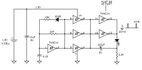
1.5V LED FLASHER CIRCUIT
AVERAGE CURRENT = 120uA
PEAK LED CURRENT = 20mA
4mS PULSE 1 FLASHE/SEC
APPROX. 6 MONTHS OPPERATION FROM N-CELL
APPROX. 12 MONTHS OPPERATION FROM AA CELL
DAVID JOHNSON AND ASSOCIATES
Friday, October 17, 2014
Radio only 1 transistor without electricity
Experts and amateurs have been Experimenting with radios without batteries since the wireless communication started.
In many designs weve seen radios that operate without power, but all are known to use the diode 1N34. (Crystal Radio).
In many designs weve seen radios that operate without power, but all are known to use the diode 1N34. (Crystal Radio).
Although significant improvements have increased the sensitivity and selectivity of these system circuits, Performances were limited until new techniques have emerged.
Here we have the first transistor radio that works without batteries, it is powered by random electric fields are everywhere in the atmosphere.
These circuits are relatively cheap to manufacture, have more volume and better reception from the crystal radios.
This circuit is a medium wave receiver and attaches easily to frequencies from 500Khz to 11Mhz.
To get good results in the reception of radio stations, we should give great importance to the ground and the antenna.
To listen to distant and weak stations we have to use a battery 9volt parallel with the capacitor C4 with its positive side between R2 and C4.
The coils are in the frequency of 500-1500Khz is tight and closely wrapped.
The coils are in frequency of 1.5-11Mhz is more tighter and more closely wrapped.
12v Battery Charger Circuit
The circuit may be accustomed charge 12V lead acid batteries.
Overview
Overview
Pin one of the LM317 IC is that the management pin that is employed to manage the charging voltage, Pin a pair of is that the output at that the charging voltage seems, Pin three is that the input to that the regulated DC offer is given.
The charging voltage and current is controlled by the electronic transistor (Q1), electrical device (R1) and POT (VR1). once the battery is 1st connected to the charging terminals, the present through R1 will increase. This successively will increase the present and voltage from LM317. once the battery is totally charged the charger reduces the charging current and also the battery are charged within the trickle charging mode.
The charging voltage and current is controlled by the electronic transistor (Q1), electrical device (R1) and POT (VR1). once the battery is 1st connected to the charging terminals, the present through R1 will increase. This successively will increase the present and voltage from LM317. once the battery is totally charged the charger reduces the charging current and also the battery are charged within the trickle charging mode.
Circuit

Notes
- The input voltage to the circuit should be a minimum of 3V more than the expected output voltage. luminous flux unit 317 dissipates around 3V throughout its operation. Here I used 18V DC because the input.
- The charging voltage may be set by victimization the POT (VR1).
- The luminous flux unit 317 should be mounted on a sink.
- All capacitors should be rated a minimum of 25V.
- Youll be able to use crocodilian clips for connecting the battery to the charger.
A Simple Function Generator

This is a simple function generator circuit that can produce the following waveforms: square wave, triangular wave, and sine wave.
The circuits main components are two 1458 ICs. The 1458 is a dual op-amp IC, i.e., an IC that houses two op amps inside it. The circuit uses four op amps, two from each 1458.
The bottom-most op amp in Figure 1 is configured as an astable multivibrator, which continuously generates a square wave. Assume that C1 has no charge initially. The voltage at the inverting input is zero, while the voltage at the non-inverting input is very slightly positive (a ratio of the op amps output offset voltage as determined by R1 and R2). This minute voltage difference at the inputs is enough to cause the op amps output to swing to high.
When the output becomes high, C1 starts charging up. The voltage at the inverting input soon exceeds that at the non-inverting input, forcing the output to swing to low, which discharges C1 again. At a certain point, the voltage at the non-inverting input exceeds that at the inverting input again, and the output of the op amp goes high again.
This cycle wherein the first op amps output swings between low and high goes on indefinitely, generating the square wave.
The two middle op-amps are both configured as integrators. The input to the second op amp is the square wave output of the first op amp. Being configured as an integrator, this op amp outputs a triangular wave (the integral of a square wave), as shown in Figure 1.
The triangular wave output of the second op amp is then fed into the third op amp, which is also configured as an integrator. The output of the third op amp is a sine wave (the integral of a triangular wave).
The sine wave output of the third op amp is fed into the fourth op amp, which is configured as an inverting amplifier. The output of this last op amp is also a sine wave but opposite in phase as its input.
Thursday, October 16, 2014
50W Electronic Amplifier Rise
This electronic amplifier project is an IC amplifier module from ST Microelectronics, the TDA7294. It is intended for use as a top quality audio class AB amplifier in hi-fi applications. Its low noise and distortion, wide bandwidth and nice output current capability, enabling it to supply high power in to both four ohm and 8 ohm lots. Its both short circuit and thermal protection.
With the addition of a handful of parts and an appropriate power supply, this module will deliver over 50W RMS in to four or 8 ohms-with < 0.1% Total Harmonic Distortion (THD) and < 0.1% Inter-modulation Distortion (IMD). It is also suitable as a replacement power amp stage, or upgrade for plenty of existing amplifiers of between 30W-50W, provided they have an appropriate dual supply, & most do.
With the addition of a handful of parts and an appropriate power supply, this module will deliver over 50W RMS in to four or 8 ohms-with < 0.1% Total Harmonic Distortion (THD) and < 0.1% Inter-modulation Distortion (IMD). It is also suitable as a replacement power amp stage, or upgrade for plenty of existing amplifiers of between 30W-50W, provided they have an appropriate dual supply, & most do.
The Specifications of the electronic amplifier project there are:
D.C. Input : 35V
Output power : > 50W RMS, 4-8 ohm load.
Gain : 24 dB (30dB modification)
Input sensitivity : one.3V for 50W, 8 ohm
Signal-to-Noise ratio : > 95 dB, (>105 dBA)
Frequency response : approx. 20Hz - 200kHz, �3 dB
Slew rate : > 10V/uS
THD : < 0.01%, 1W-40W, 1kHz
IMD : < 0.01%, 1W
D.C. Input : 35V
Output power : > 50W RMS, 4-8 ohm load.
Gain : 24 dB (30dB modification)
Input sensitivity : one.3V for 50W, 8 ohm
Signal-to-Noise ratio : > 95 dB, (>105 dBA)
Frequency response : approx. 20Hz - 200kHz, �3 dB
Slew rate : > 10V/uS
THD : < 0.01%, 1W-40W, 1kHz
IMD : < 0.01%, 1W
The maximum supply voltage of the IC is +/- 40V. However the maximum dissipation of the IC can be exceeded even at a lower voltage. Therefore the supply voltage used require not be over +/- 35V. This can be constructed using a 50V middle tapped-transformer, a diode bridge rated at 5A (min.) & a pair of electrolytic capacitors, as shown below. A lower secondary voltage transformer could even be used but the reduced DC voltage will lead to less power output in to 8 ohms. You can still receive 50W in to four ohms with only 24V supply rails.
A 36V C.T. transformer will give you approx +/- 25V rails. The-mains transformer used ought to be rated at a maximum of 80VA. In the event you require to run modules in a stereo amplifier you can use a common power supply. In this case the transformer ought to be rated at 150VA or greater.
A 36V C.T. transformer will give you approx +/- 25V rails. The-mains transformer used ought to be rated at a maximum of 80VA. In the event you require to run modules in a stereo amplifier you can use a common power supply. In this case the transformer ought to be rated at 150VA or greater.

Electronic Amplifier Circuit Diagram Description
Most of the circuitry is contained within the IC module. The input signal is applied to pin three by capacitor C1 & low-pass filter R1/C2. The filter improves the pulse response & helps cease RF signals. The lower -3dB point is determined-by R2/C1 & R4/C3. This is about 20Hz for the values used. The upper -3dB point is over 200kHz. C7/C8 & C9/C10 provide additional power supply filtering or decoupling.
![50W]()
.gif)
R3/R4 are the feedback resistors. The gain is 1+R3/R4 which is approx 16 times, or 24dB. In case you need to increase the input sensitivity you may alter the resistors to suit. Changing R3 to 22k would increase the gain to 30dB and lower the input-required for 50W in to 8 ohm, to 0.6V, without affecting performance much. In case you reduce the worth of R4 you will also need to increase C3 to maintain bass response, as this sets the feedback low frequency roll off.
Pin ten is a mute input and pin 9 provides a standby mode. Muting ought to always happen before standby mode is selected. Connecting these pins permanently to the supply rail ensures that the amplifier comes on immediately on power up. Any switch-on clicks may be eliminated by increasing the time constants of R5/C4 and R6/C5 if necessary.
Make definite that a heavy duty heat-sink rated at least one.4 degree C/W or better is used.

Sun Up Alarm circuit
The Sun-Up Alarm circuit can be used to provide a audible alarm for when the sun comes up or it can be used in a dark area and detect when a light comes on. It can also be used to detect a light beam, headlights etc. The circuit works as follows. The phototransistor is very sensitive to light. (Any phototransistor will work fine) The sun shining on this device will provide a high to one of the NAND gates. This will cause another NAND gate to oscillate which will drive another gate to output a 100hz tone. The transistor provides drive for the speaker.
Source
Read More..
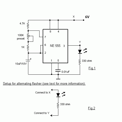
SourceNew Light Flasher Circuit Diagram
This is a very basic circuit for flashing one or more LEDS and also to alternately flash one or more LEDs.It uses a 555 timer setup as an astable multivibrator with a variable frequency.With the preset at its max. the flashing rate of the LED is about 1/2 a second. It can be increased by increasing the value of the capacitor from 10uF to a higher value.
For example if it is increased to 22uF the flashing rate becomes 1 second. There is also provision to convert it into an alternating flasher. You just have to connect a LED and a 330ohm as shown in Fig.2 to the points X and Y of Fig.1. Then both the LEDs flash alternately.Since the 555 can supply or sink in upto 200mA of current, you can connect upto about 18 LEDS in parallel both for the flasher and alternating flasher (that makes a total of 36 LEDs for alternating flasher).
Light Flasher Circuit Diagram
Wednesday, October 15, 2014
Simple 8 Channel DTMF Link Encoder
Generated millions of times every day by our telephone keypads, the eight DTMF frequencies were chosen so that the harmonics and intermodulation do not generate significant in-band signal levels. The signal is encoded as a pair of sine waves, ensuring that no frequency is a multiple of the other and the sum and difference between two frequencies does not match any single tone and that’s why DTMF sounds so ugly!T he DTMF encoder circuit show n here is based on the HT9200B tone generator device produced by Holtek and distributed by Futurlec among others. The encoder is complemented by a decoder elsew her e in this publication.
8-Channel DTMF Link: Encoder Schematic

The HT2900B is supplied as a nice old fashioned 14-pin device. It can be instructed by a microcontroller to generate 16 dual tones and (in serial mode only) 8 single tones from the DTMF pin output . It s 8 - pin ‘ younger brother’ the HT9200A provides a serial mode only whereas the HT9200B contains a select-able serial/parallel mode interface for various applications such as security systems, home automation, remote control through telephone lines, communication systems, etc.
A 74HC148 8-to-3 priority encoder is used to convert the ‘keypad’ information from S1–S8 into 3-bit tone selection words the HT9200B wants to see at its input. The ninth switch, S9, is connected to input D3 on the encoder chip. Pressing one of the switches S1–S8 generates a complementary 3-bit binary word at outputs A0, A1, A2 of IC1. IC2 then generates the dual tones accordingly to these binary codes.
Pressing S1–S8 generates the dual tones for DTMF digits C, B, A, #, *, 0, 9 and 8. By pressing and holding down S9 the DTMF digits 7, 6, 5, 4, 3, 2, 1 and D are generated.
To generate the eight single frequencies accurately a 3.58 MHz crystal quartz is connected to pin 2 and 3 of IC2. Pin 13 of the HT9200B supplies a DTMF signal of about 150 mV at a 5 KO load.
Pull-up resistor array R2 may be omitted if you substitute the 74HC148 with a 74LS148. R1 must be present in that case, otherwise it can be omitted.
Simple Luggage Security Alarm Schematic
We usually lock our luggage utilizing a chain-and-lock arrangement when in travelling by a train of bus. But, still we are worried, apprehending that someone may possibly break the chain and steal our luggage. The following schematic is really a very simple and easy build luggage security alarm circuit to alert you when a person tries to break the chain.

Transistor T1 allows supply to the sound generator chip when the base current begins flowing through it. When the wire (thin enameled copper wire of 30 to 40 SWG, applied for winding transformers) loop around the chain is cracked by someone, the base of transistor T1, which was previously linked with positive rail, becomes opened. Because of this, transistor T1 gets forward biased to extend the positive power source towards the alarm circuit.
In idle mode, the power source consumption within the circuit is lowest and as a result, it could possibly be utilized for numerous travel hrs.
To make it possible for generation of various alarm sounds, joints to pin 1 and 6 could be designed as shown in the following table:

In idle mode, the power source consumption within the circuit is lowest and as a result, it could possibly be utilized for numerous travel hrs.
To make it possible for generation of various alarm sounds, joints to pin 1 and 6 could be designed as shown in the following table:

Monday, October 13, 2014
Boost up current to 8 Amps from a LM2575
The LM2575 works a regulator only and don’t deliver any current to the load.
If the regulator switches “ON”, you find a voltage at the output of it. This makes T4 switching on also.
The collector of T4 now is nearly GND and also the Gate of FET T3. This FET switches on (it’s a P-FET!)
For T3 you can take everything what’s called Power P-FET with low RDSON, a IRF9540 is a good choice.
The “invention” of this circuit is the Gate turn off of T3.
In ON State, The Gate of T3 has nearly GND potential, D9 conducts and T5 is off.
If now the Regulator switch it’s output OFF, then the Base of T4 is pulled low by R12 and no currents flow through T4.
Also the cathode of D9 is connected to Vcc via R13. The stored energy in the Gate capacity of T3 lets now pull T5′s emiter lower then the base. Whats happens if the Base of a NPN transistor has higher voltage than the emiter? It conducts ! Now, T3′s gate is directly connected to the source via T5 and the gate capacity can be discharged very fast.
DIY Digital Thermometer in Wireless Form Overview and explanation
Overview
This digital thermometer project uses any standard FM broadcast band radio at regular intervals in order to report the temperature.
Explanation
An Atmel AT90S1200 is used to construct the prototype along with a modified low cost wireless microphone kit that function as the transmitter in order to save design time. The device can be used as standalone or as part of a PC-based weather station or HVAC system since it uses a simple low bit rate tone signaling scheme which can be interpreted easily by both machines and humans. The design allows the use of any inexpensive FM radio to monitor the temperature with easy set up of any number of monitoring locations.
There are various circuits used in this project including, the thermometer interface, audio interface, and power interface. The operation consists of applying power and tuning the unit to any unused FM channel. A 9V transistor radio battery was chosen since the 5V regulator used can accept any DC voltage between 5.5V-12V. A programs tests if larger or lesser and converts the binary format temperature output from the thermometer clip to a format that can be transmitted a digit at a time.
Akrapovic Twin Exhaust System Schematic Diagram for 2009 SUZUKI GSX R 1000
Akrapovic Racing and Evolution systems are designed for riders who demand maximum performance from their motorcycle. Both systems are significantly lighter if compared to stock exhaust system and feature exceptional production quality, hi-tech materials and of course increased engine performance combined with pure racing sound output. 
The following file contains detail description and explanation on Akrapovic Twin Exhaust System for 2009 SUZUKI GSX-R 1000 and its schematic diagram. The system’s effect on the torque and power curve is huge and strongest in midrange rpm.
Get more info on Akrapovic Twin Exhaust System Schematic Diagram for 2009 SUZUKI GSX-R 1000 here
Friday, October 10, 2014
Mini stereo circuit using ic TDA2822
This circuit IC1 TDA2822 number as your primary device. The Dual Amplifier IC or IC stereo gain at 40 dB. Bandwidth 120 kHZ. That is about 2 watts and watt power supply of 1.8 to 15 volts and a current 6 mA only
When using the power supply 9 volt into this circuit.VR1 and VR2 to adjust the signal level of the right and left, the pin 7 and pin 6 of IC1.The amplifier IC1 is out of the output pin 1 and pin 3, through the C4 and C5 coupling signals to the left and right speakers.The C6, R1 and C7, R2 is to reduce noise.
LM317 variable power supply
Description:
A truly timeless circuit. LM317 is a versatile and highly efficient 1.2-37V voltage regulator that can provide up to 1.5A of current with a large heat sink. Its ideal for just about any application. This was my first workbench power supply and I still use it.
Since LM317 is protected against short-circuit, no fuse is necessary. Thanks to automatic thermal shutdown, it will turn off if heating excessively. All in all, a very powerful (and affordable!) package, indeed.
Although LM317 is capable of delivering up to 37V, the circuit pictured here is limited to 25V for the sake of safety and simplicity. Any higher output voltage would require additional components and a larger heat sink.
Make sure that the input voltage is at least a couple of Volts higher than the desired output. Its ok to use a trimmer if youre building a fixed-voltage supply.
Problems:
Follow all the safety precautions when working with mains voltage. Insulate all connections on the transformer.
Possible uses:
Variable workbench power supply, fixed-voltage supply... Just about any possible application when no more than 1.5A is necessary.
read more at: http://english.cxem.net/power/power8.php
Thursday, October 9, 2014
Solar Power walkway marker Led display
These are the little lights with the stake on the bottom that you can push into the ground along your driveway or sidewalk and have the solar panel on top. The solar cell charges a AA NiCd battery during the day and at night the battery powers the LED. The circuit board in this particular model was originally designed to hold a pair of 5mm amber LEDs, but the manufacturer apparently found a source of higher power 10mm amber LEDs and the final product only needs one of these. Due to the limited space, many of the components are surface mount. The transistors are both 2N3904 equivalent surface mounts. Unfortunately, the capacitor is also surface mount and is unmarked.
The charging circuit is fairly simple and has a photovoltaic solar cell to charge the battery and a diode to prevent the battery from powering the cell when it’s dark. Now moving along, there is a cadmium sulphide (CdS) photo resistor, a 10k resistor and a 1k resistor that forms a voltage divider at the base of Q1. When light hits the photo resistor, it has a low resistance which is amplified by the transistor. The collector is tied to the base of the left hand transistor, so when it’s on it clamps its base to ground and prevents it from oscillating. When it’s dark and the CdS Cell has a high resistance, the right transistor is off which allows the rest of the circuit to begin oscillating.
Touch Switch Circuit with explnation
This electronic circuit uses a 555 timer as the bases of the touch switch. You can learn more about 555 timers in the Learning section on my site. When the plate is touched the 555 timer is triggered and the output on pin 3 goes high turning on the LED and the buzzer for a certain period of time. The time that the LED and the buzzer is on is based on the values of the capacitor and resistor connected to pin 6 & 7. The 10M resistor on pin 2 causes the the circuit to be very sensitive to the touch.

Wednesday, October 8, 2014
New FM Stereo Transmitter BH1415F
BH1415F can be supplied with 6 - 15V voltage, consumes only around 25mA while providing very sound quality and improved 40dB channel separation. BH1415 is only available in SOP22 IC case and this may be an inconvenience for some folks. On the other hand, because the chip is smaller than regular DIP-based ICs it is possible to fit the entire stereo coder on a small PCB.

Subscribe to:
Posts (Atom)