


Detects clipping in preamp stages, mixers, amplifiers etc., Single LED display – 9V Battery supply unit
This circuit was intended to be used as a separate, portable unit, to signal by means of a LED when the output wave form of a particular audio stage is “clipping” i.e. is reaching the onset of its maximum permitted peak-to-peak voltage value before an overload is occurring. This will help the operator in preventing severe, audible distortion to be generated through the audio equipment chain. This unit is particularly useful in signaling overload of the input stages in mixers, PA or musical instruments amplification chains, but is also suited to poweramplifiers. A careful setting of Trimmer R5 will allow triggering of the LED with a wide range of peak-to-peak input voltages, in order to suit different requirements. Unfortunately, an oscilloscope and a sine wave frequency generator are required to accurately setup this circuit. Obviously, the unit can be embedded into an existing mixer, preamp or power amplifier, and powered by the internal supply rails in the 9 – 30V range. The power supply can also be obtained from higher voltage rails provided suitable R/C cells are inserted. SW1 and B1 must obviously be omitted.
Circuit diagram:
Parts:
R1_______________1M 1/4W Resistor (See Notes)
R2,R3,R8_______100K 1/4W Resistors
R4,R6___________10K 1/4W Resistors
R5_______________5K 1/2W Trimmer Cermet or Carbon
R7_______________2K2 1/4W Resistor
R9______________22K 1/4W Resistor
R10______________1K 1/4W Resistor (See Notes)
C1,C4__________220nF 63V Polyester Capacitors
C2_______________4p7 63V Ceramic Capacitor (See Notes)
C3_____________220µF 25V Electrolytic Capacitor
C5______________10µF 25V Electrolytic Capacitor (See Notes)
D1,D2________1N4148 75V 150mA Diodes
D3______________LED (Any dimension, shape and color)
Q1____________BC547 45V 100mA NPN Transistor
IC1___________TL062 Dual Low current BIFET Op-Amp (or TL072, TL082)
SW1____________SPST Toggle or Slide Switch (See Text)
B1_______________9V PP3 Battery (See Text)
Circuit operation:
The heart of the circuit is a window comparator formed by two op-amps packaged into IC1. This technique allows to detect precisely and symmetrically either the positive or negative peak value reached by the monitored signal. The op-amps outputs are mixed by D1 and D2, smoothed by C4, R7 and R8, and feed the LED driver Q1 with a positive pulse. C5 adds a small output delay in order to allow detection of very short peaks.
Notes:
Output power: 6W into 4 Ohm load, FET input stage – Passive Tone Control
Tiny, portable Guitar Amplifiers are useful for practice on the go and in bedroom/living room environment. Usually, they can be battery powered and feature a headphone output. This project is formed by an FET input circuitry, featuring a High/Low sensitivity switch, followed by a passive Tone Control circuit suitable to Guitar or Bass. After the Volume control, a 6W IC power amplifier follows, powered by a 12-14V dc external supply Adaptor or from batteries, and driving a 4 Ohm 10 or 13cm (4″/5″) diameter car loudspeaker. Private listening by means of headphones is also possible.
Circuit diagram:
Parts:
P1______________1M Linear Potentiometer
P2____________100K Log Potentiometer
R1_____________68K 1/4W Resistor
R2____________470K 1/4W Resistor
R3______________2K7 1/4W Resistor
R4______________8K2 1/4W Resistor
R5____________680R 1/4W Resistor
R6____________220K 1/4W Resistor
R7_____________39R 1/4W Resistor
R8______________2R2 1/4W Resistor
R9____________220R 1/4W Resistor
R10_____________1R 1/4W Resistor
R11___________100R 1/2W Resistor
R12_____________1K5 1/4W Resistor
C1____________100pF 63V Polystyrene or Ceramic Capacitor
C2,C5,C9,C14__100nF 63V Polyester Capacitors
C3____________100µF 25V Electrolytic Capacitor
C4_____________47µF 25V Electrolytic Capacitor
C6______________4n7 63V Polyester Capacitor
C7____________470pF 63V Polystyrene or Ceramic Capacitor
C8______________2µ2 25V Electrolytic Capacitor
C10___________470µF 25V Electrolytic Capacitor
C11____________22nF 63V Polyester Capacitor
C12__________2200µF 25V Electrolytic Capacitor
C13__________1000µF 25V Electrolytic Capacitor
D1______________3mm red LED
Q1____________BF245 or 2N3819 General-purpose N-Channel FET
IC1_________TDA2003 10W Car Radio Audio Amplifier IC
SW1,SW2________SPST toggle or slide Switches
J1____________6.3mm Mono Jack socket
J2____________6.3mm Stereo Jack socket (switched)
J3_____________Mini DC Power Socket
SPKR__________4 Ohm Car Loudspeaker 100 or 130mm diameter
| Elektor 303 Circuit |
| Practical Arduino |
| Elektor05-2010 |
| Elektor05-2010 |
| Elektor05-2010 |
| Nuts Volts 06-2010 |
| Nuts Volts 06-2010 |
source: http://electronicsprojects.mediadir.in/mini-guitarbass-amplifier/
Notes:
Technical data:
Output power (1KHz sinewave):
6W RMS into 4 Ohm at 14.4V supply
Sensitivity:
50mV RMS input for full output
Frequency response:
25Hz to 20kHz -3dB with the cursor of P1 in center position
Total harmonic distortion:
0.05 – 4.5W RMS: 0.15% 6W RMS: 10%
Tone Control Frequency Response:
 |
| 1000W Power Amplifier |


 |
| 2 x 32W DUAL BRIDGE CAR RADIO AMPLIFIER |


Part Total Qty. Description

C1 1 10uF 16V Electrolytic Capacitor
R1, R2 2 100K 1/4 Watt Resistor
R3 1 10 Meg 1/4 Watt Resistor
U1 1 4011 CMOS NAND Gate IC
MISC 1 Board, Wire, Socket For U1
 In the development and research of electronic equipment in the laboratory one of the most important components of the measurement equipment is a universal source of test signals. Function generator, working in a range of sound frequencies, was developed based on a microcontroller. It is based on generator circuit described in [Radiohobby, 2000, № 5, p. 79]. The analysis of this scheme it was revealed a significant disadvantage. Because the counter is formed by two functional elements, the logic levels on the address pins are not installed simultaneously, which leads to the appearance of high-frequency emissions of the generator output. Developed device devoid of these deficiencies. Generated output waveform (saw, triangle, sine, square wave) programmed in flash-memory. The generator used firmware contained in [Radiohobby, 2000, № 5, p. 79]. Schematic diagram of the function generator is shown in Fig. 1.
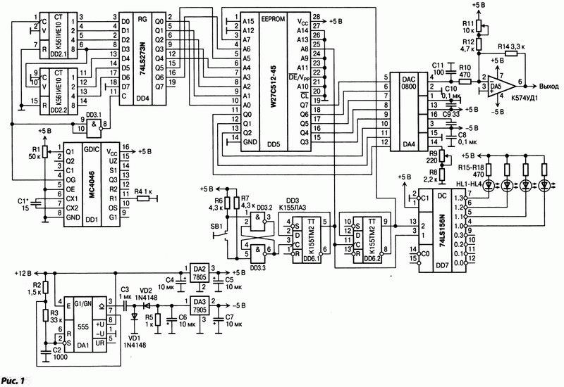
| Wireless Audio Power Amplifier Transmitter Circuit Diagram |
 |
| Wireless Audio Power Amplifier Transmitter Circuit Diagram |